Top Links
Journal of Materials Science and Nanotechnology
ISSN: 2348-9812
Characterizations of Cu2FeSnSe4 Thin Films Synthesized from Nanoparticles Powder
Copyright: © 2024 Louardi Yandjah . This is an open-access article distributed under the terms of the Creative Commons Attribution License, which permits unrestricted use, distribution, and reproduction in any medium, provided the original author and source are credited.
Related article at Pubmed, Google Scholar
Cu2FeSnSe4 (CFTSe) thin film were synthesized on glass substrate by thermal evaporation method at Ts=400° C, starting from elemental powders mixed by a mechanical alloying process. The structural, morphological, compositional, optical and electrical properties of CFTSe semiconductor have been investigated by X-ray diffraction (XRD), Raman spectroscopy, scanning electron microscopy (SEM), transmission electron microscopy (TEM), energy dispersive X-ray analysis (EDAX), spectroscopic ellipsometry (SE) and Van Der Pauw technique, respectively. The morphology and chemical composition of the (CFTSe) microparticles have been confirmed by the scanning electron microscope (SEM) and energy dispersive spectrometer (EDS). XRD results showed that the film has a polycrystalline nature with cubic structure and a lattice parameter α =5.682 Å with a texture along the (111) plane. The optical constants and dielectric parameters were found between 1.00 to 5.00 eV, the optical absorption coefficient (α) was above 6.5×103 cm-1 and the band gap were found at Eg = 1.60 eV. The thin film presented a hole density of 1.646×10⁹ (cm-3), a hole mobility of 2.709x10²(cm2 V-1 s-1 and an electrical conductivity of 7.146×10² (Ω-1.cm-1).
Keywords: Cu2FeSnSe4; Mechanical Alloying; Nanoparticles; Thin Films; Thermal Evaporation; Semiconductor Cubic Structure
Stannite-group minerals have attracted substantial research interest due to their potential application in solar cells, thermoelectric, optoelectronics and energy storage. Cu2FeSnS4 (CFTS) and Cu2FeSnSe4 (CFTSe) are considered to be amongst the better solar cell materials; they contain earth abundant elements with high absorption coefficient and have good stabilities.
The scarcity of natural energy sources combined with the polluting conventional energy production make the scientific community looking for alternative sustainable energy sources. In this context, the search for new materials and methods in photovoltaic by production of thin films with low cost has been stimulated [1]. Different types of semiconductor materials have received great interest especially Se-based absorbers due to their relative abundance at reasonable cost and their attractive optoelectronic properties, such as CISe, CIGSe, CTSe and CZTSe [2]. More recently, some researchers were interested in studying quaternary semiconductors such as CFTSe and CZTSe because they are characterized by their interesting range gap, inexpensive, non-toxic and having high absorption coefficients [3]. In solar cell technology, CFTSe is considered a promising alternative to conventional materials like silicon and cadmium telluride. The material's optimal bandgap (around 1.0-1.2 eV) allows it to absorb a broad spectrum of sunlight, enhancing its efficiency in converting solar energy into electricity. In the field of thermoelectrics, CFTSe exhibits potential for waste heat recovery and power generation applications. A good thermoelectric material should have a high Seebeck coefficient, low thermal conductivity, and high electrical conductivity.
In addition, thin films of Cu2FeSnSe4 can be synthesized using various methods, including physical vapor deposition (PVD) techniques such as co-evaporation or sequential deposition [4], selenization of RF magnetron sputtered precursors [1], reaction time of selenization [5], a simple solvothermal method [6], chemical spray pyrolysis [7].
In this present work, we present a complete study focused on a Cu2FeSnSe4 thin film grown by thermal evaporation whose advantages are its efficiency, simplicity, low cost, weak impact on the physical properties of the target material and allowing a good control of the film thickness with a nanometer size accuracy [8]. (CFTSe) thin film was prepared by thermal evaporation process offers advantages such as simplicity and compatibility with various substrate materials. However, it may have limitations regarding uniformity and control over stoichiometry in complex compound systems like Cu2FeSnSe4. The optimization of process parameters is necessary to achieve desired film properties. The composition, structure, morphology and electro-optical proprieties of CFTSe thin film were studied. The results suggest that Cu2FeSnSe4 semiconductors are promising candidates for solar cells.
In summary, the synthesis and characterization of Cu2FeSnSe4 thin films play a crucial role in advancing solar cell technology, thermoelectric, and other relevant fields by optimizing material properties, improving device performance, and expanding the range of potential applications. These efforts contribute to the development of sustainable energy solutions and innovative technologies with broad societal and economic impacts.
In the experimental section of the study, crucial parameters such as deposition rate during thermal evaporation, annealing conditions, and the purity of starting materials play significant roles in determining the properties of the synthesized Cu2FeSnSe4 ( CFTSe) thin films.
Cu2FeSnSe4 thin film was synthesized by a simple step process. Copper, Iron, Tin and Selenium as pure starting components (Cu, Fe and Sn granular, 99.99%, from Balzers) and (Se pellets, 99.99%, from Balzers) were weighted to reach the following molar proportion of Cu: Fe: Sn: Se/2:1:1:4 and they were milled using high energy planetary ball mill (Fritsch premium line P-7) [9]. The powder/balls weight ratio was 1/2 with a rotational speed of 300 rpm and a milling time of 3 hours and 30 minutes. The resulting nano powder was employed to produce Cu2FeSnSe4 thin film were grown by thermal evaporation onto pre-cleaned glass substrates and on (100)-oriented Si wafers doped with 1015/cm3 of boron substrates; This technique as described in detail elsewhere [10] under vacuum at about 10-6 Torr and the substrates temperature was fixed at Ts=400°C. The deposition rate measured by a quartz crystal microbalance for thin film deposition was 150 Å/s for thermal evaporation.
Structural properties of the powders and the films were investigated by X-ray diffraction (XRD) using Philips Xpert NPD Pro diffractometer equipped with a Cu-Kα radiation λ=1.54187 Å, in the range of 2θ between 10° and 100° with a step size value of 0.02° and a counting time of 2s. Furthermore, to identify the possible secondary phases in the fabricated films, Raman spectroscopy was performed using a Spectro Raman system equipped with a confocal Horiba Jobin-Yvon T64000 spectrometer and a laser source of excitation wavelength λ=632.8 nm. Characterization techniques assist in optimizing synthesis parameters thereby enhancing material performance and stability for various applications. The synthesis and characterization of CFTSe thin films are crucial for advancing solar cell technology, thermoelectric and other fields, promoting efficient and sustainable energy conversion.
The characterization of surface morphology was performed by scanning electron microscopy (SEM) and the chemical composition was determined by energy dispersive X-ray spectrometry (EDAX) installed in a JEOL6400 SEM microscope (JEOL Ltd, Tokyo, Japan). Transmission electron microscopy (TEM) was used to investigate the microstructure of the samples and the microscope employed was a 2010 FEG JEOL microscope operated at 200 keV.
The optical properties of the CFTSe thin films were analyzed by spectroscopic ellipsometry (SE) using a phase modulation ellipsometer. The data were collected while the incident light was scanned between 1.5 eV and 5.0 eV with steps of 0.02 eV at the incident angle of 66.2°. This was carried out by means of a Jobin–Yvon Ellipsometer (UVISEL). Hall concentration, Hall mobility and the resistivity measurements were determined at room temperature by the Van Der Pauw technique.
A typical X-ray diffraction (XRD) pattern of the Cu2FeSnSe4 nano powder is shown in Figure1. The observed peaks with high intensities corresponding to (111), (220), and (311) planes at values of angles 2θ=27.18°, 45.15°, 53.51° and lower intensities at (400), (331), (422), and (511) planes with 2θ values of 65.61°, 72.56°, 83.26° and 89.68°, respectively indicate that CFTSe has a cubic structure with a lattice parameter a=5.682Å which is consistent with the standard pattern of Cu2FeSnSe4 (PDF file #27-0167). This result is in good agreement with previous works on this material according to [11]. However, we notice a very small peak at 2θ= 30.71° corresponding to an interreticular distance (d=2.90 Å), which originates from a ternary phase Cu2SnSe3 (PDF file #89-2879) meaning that this phase is in a very small quantity in the powder.
The morphology of the CFTSe milled powder is illustrated by an SEM view presented in Figure2.a with a large cluster (up to 200 µm diameter) of agglomerated grains, the inset in the top right-hand side is an enlargement of the corresponding image centered on one of these clusters. The compositional analysis of the obtained from EDS spectroscopy is Cu: 28.01 at. %, Fe: 5.13 at. %, Sn: 13.18 at. % and Se: 53.68 at.%. Obviously, our sample is iron and tin-lacking due to the mechanical alloying process (see Figure2.b).
The crystallite size of CFTSe powder was estimated from the most intense (111) and (220) peaks to be 24.74 nm using Debye Scherer’s formula [12,13]:
Where D is the average crystallite size, k is the shape factor (k=0.9), λ is the X-ray diffraction wavelength (λ=1.54187Å) and βhkl is the full width at half maximum (FWHM) of the corresponding peak position in radian.
In order to determine the value of the dislocation density (δ), we used Williamson and Smallman's formula [14]:
The estimated value of the dislocation density for the deposited powder was found to be
Moreover, for a better characterization, the crystallite size (D) and the lattice strain (ε) induced in the CFTSe powder were calculated using the Williamson’s and Hall’s formula equation as indicated below [15]:
The Scherrer's formula for crystallite size and the micro strain terms are both included in the Hall-Williamson equation.
Figure3. shows that (D) and (ε) can be calculated from the slope and y-axis intercept of βhkl cosθhkl versus 4sin θhkl plots, respectively. The values are given in Table 1. The positive residual strain value for the Cu2FeSnSe4 nanoparticles indicates that it is the extension strain.
The crystal structure of the CFTSe powder was also analyzed by means of TEM observations. A selected area electron diffraction (SAED) shown in Figure4. (a) confirms the presence of the crystalline CFTSe phase with the distinct planes corresponding to the (111), (220), (311), (400), (331), (422) and (511) planes of a cubic structure having a lattice parameter value of 0.568 nm which are in good agreement with the XRD data. Interestingly, the two circled diffraction points correspond to iron (Fe). Figure4. (b) shows a typical dark field TEM image and brings the evidence of the crystalline nature of the grains. A high-resolution transmission electron microscope (HREM) image of the CFTSe powder is shown in Figure4. (c) from which one can measure an interplanar spacing d= 0.207 nm. This value is in good agreement with the (111) d spacing of the iron cubic structure (d011= 0.207 nm). At last, the corresponding Fast Fourier transform (FFT, Figure4. (d)) of the HREM image confirms the cubic structure of the grain since it is consistent with a [1,1,0] projection.
Cu2FeSnSe4 thin films were synthesized by thermal evaporation technique on a glass substrate temperature and at Ts=400°C. Figure5. shows the X-ray diffraction (XRD) pattern of the CFTSe film. It can be seen that the sample is composed of three phases. Firstly, a quaternary cubic phase whose XRD peaks are located at 2θ =26.61°, 44.04°, 56.45°,61.85°, 75.65°, 90.02°, and corresponding to interplanar d spacing 3.35Å, 2.05Å, 1.63Å, 1.50Å, 1.26Å, 1.09Å, respectively.
These peaks are identified from reflections of (111), (220), (311), (400), (331), (511), which was compared with the interplanar d spacing of Cu2FeSnSe4 (PDF file #27-0167). Secondly, Cu2SnSe3 ternary cubic phase with peaks at 2θ =31.23°, 33.16°, 66.55°, 66.20°, corresponding to 2.87Å, 2.70Å, 1.41Å, 1.35Å distances, respectively and they are identified from reflections of 200, 220, 400, 331 lattice planes, which are in good agreement with the PDF file #89-2879. Finally, binary phases are observed such as SnSe at 2θ =25.46°, 29.58°, 30.57°, 37.80°, 47.79°, 49.89°, 52.23°, 54.60°, 91.08° and Cu2Se at 2θ =13.09°, 25.38°, 52.18°. They correspond well with PDF files #32-1382, #35-1042 and PDF file #19-0401, respectively.
In this work the Full Width at Half Maximum (FWHM) of the 111, 220,and (311) peaks in the CFTSe thin film. The FWHM values obtained were 2θ =31.23°, 33.16°and 66.55°, respectively. These values indicate that the as-synthesized thin film possesses excellent crystallinity. Moreover, the average grain size was calculated to be 24 nm using the Scherrer equation.
The Raman spectra analysis provides valuable information not only about the structure of the CFTSe thin film but also about the presence of other compounds such as Cu2SnSe3, CuxSe, and SnSe2 within the synthesized CFTSe. This is because the most intense X-ray diffraction (XRD) peaks of these compounds coincide with those of CFTSe. Raman spectra not only can describe the structure of CFTSe thin film but also can detect the presence of Cu2SnSe3, CuxSe and SnSe2 in the synthesized CFTSe as the most intensive XRD peaks of these compounds coincide with those of CFTSe.
In addition, Raman scattering analysis was used as a complementary tool of XRD data to confirm the presence of different phases present in the film. As demonstrated by Figure6, five main peaks were found at 58 cm-1, 67cm-1, and 228 cm-1 and they can be attributed to Cu2SnSe3 [16]; 106 cm-1, 175 cm-1 can be assigned to SnSe and FeSe2 phases [7,4], respectively (see Figure6. below).
Figure7.a shows is an SEM image of a cross sectional view of the film. It provides an idea of the surface morphology of the film whose average thickness is about 950 nm. The inset shown at the top right-hand side is a top view of the film with a lower magnification. The crystallite size is well visible and it shows small spherical grains. ImageJ software (see histogram below in Figure7.b) statistic confirmed the average grain size. This value is represented by the peak position of the Gaussian curve of the histogram xc =0.2 μm.The surface of CFTSe thin film is Dense and no voids. Some information on grain sizes and crystallinity of the sample can be directly got by means of SEM. Notably, the SEM analysis reveals a grain size of approximately 200 nm, which is larger than the value calculated using the Scherrer equation. This finding is consistent with the observations made by Salome et al. [17], who also reported similar differences in their research.
In addition, Figure7.c presents an EDX spectrum of the CFTSe deposited film. The average chemical composition ratio is Cu: 59.53at. %, Fe: 0.98 at. %, Sn: 3.94at. % and Se: 35.54 at.%. This quantitative analysis is the result of various measurements from different regions on the Cu2FeSnSe4 film surface. Evidently, we can notice that the Cu-rich composition (i.e., Cu / (Fe+Sn+Se>1) of our sample is not close to the expected stoichiometry of 2:1:1:4.
The SE spectra consist in the measurement of ψ and ∆ ellipsometric angles defined from the fundamental equation of ellipsometry [18]:
Where ρ is the complex ratio of rp and rs, rp and rs being the complex reflection coefficients for parallel and perpendicular polarizations of the light, respectively. The measurement can be performed as a function of wavelength and angle of incidence.
Optical constants of interest, namely, the refractive index (n), extinction coefficient (k) as function of photon energy (eV) (see Figure8) and the thickness of CFTSe deposited film on (100) oriented silicon substrate was analyzed by spectroscopic ellipsometry (SE) technique using phase modulation ellipsometer. This method is extremely accurate and does not request a reference material.
The optical response to incident photon energy is represented by a complex dielectric function denoted by: ε=ε1+iε2
Dielectric parameters (ε1, ε2), the real part and the imaginary part respectively, were evaluated using Eq (5), (6) below [19].
The real part of the dielectric constant indicates how much the material will slow down the speed of light, while the imaginary portion describes how a dielectric material absorbs energy from an electric field due to dipole motion. The results are shown in Figure9.a:
The absorption coefficient (α~ 6.5×103cm-1) and normal-incidence reflectivity (R) for CFTSe films see Figure9.b were defined as follows [20, 21], respectively:
Where (k) is the extinction coefficient, (λ) is the wavelength and (n) is the refraction index.
The large absorption coefficient of CFTSe makes these materials very suitable as absorber materials in thin-film solar cells, and is in accord with the conditions of the solar cell absorption layer [22,23,24].
The values of n, k, ε1, ε2, R and α are in good agreement with data reported elsewhere [25,26], but the difference remains in the maximum and minimum values. This variation most likely results from the preparation process or from the presence of iron in the film. Additionally, the optical conductivity was obtained using Eq (9) below [27]:
Where σ is the optical conductance, c is the velocity of the radiation in the space, n is the refractive index and α, the absorption coefficient. The variation of the optical conductance with the incident photon energy of CFTSe film is illustrated in Figure 10 where, the highest value is ≈3.65×108cm-1.
The energy gap of the Cu2FeSnSe4 thin film was studied using Tauc’s relation presented by [28]:
Where A is a constant, α the absorption coefficient, (hν) the photon energy and Eg the optical band gap energy. The value of n is 1/2 for direct transition and 2 for indirect transition [28].
Figure 11 shows the plot of (αhν)2 versus hν and the optical bandgap of the CFTSe film can be analyzed by linear extrapolation of the line to the energy axis and the optical band gap value is found to be Eg =1.60 eV [29].
At last, electrical properties for the CFTSe thin film were analyzed. Hall concentration, Hall mobility and electrical conductivity were determined at room temperature by the Van Der Pauw technique and have been found to be 1.646x10¹⁹ (cm-3), 2.709x10² (cm2 V-1s-1) and 7.146x10² (Ω-1.cm-1), respectively. These electrical measurements confirmed the p-type nature of the film.
The main contributions of the study involve the successful synthesis and characterization of Cu2FeSnSe4 (CFTS) thin films using a mechanical alloying process and thermal evaporation technique. Structural analyses reveal that the CFTS powder consists of crystallites with an average size of 24.74 nm and a cubic structure, with a lattice parameter a = 5.682 Å. A small amount of the (Cu2SnSe3) ternary phase was also observed. The crystallite size was estimated using both Debye Scherer's and Williamson–Hall methods.
CFTS thin film was prepared at a substrate temperature of 400°C, resulting in the formation of quaternary Cu2FeSnSe4, ternary (Cu2SnSe3), and binary (SnSe, FeSe2) phases. X-ray diffraction studies confirmed the cubic structure with a (111) texture, while Raman spectra supported this behavior and revealed persistent modes of the various phases.
Optical properties of the CFTS semiconductor show a high absorption coefficient (α~ 6.5×103cm-1) and an optical band gap of Eg=1.60 eV.
This study investigates the synthesis and characterization of CFTS thin films, examining phase formation and optical properties. The findings contribute to the development of efficient and sustainable energy conversion solutions, establishing CFTS as a promising material for optoelectronic applications.
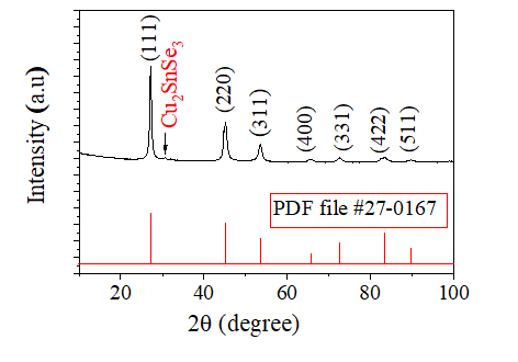 |
| Figure 1: XRD pattern of the Cu2FeSnSe4 nanopowder |
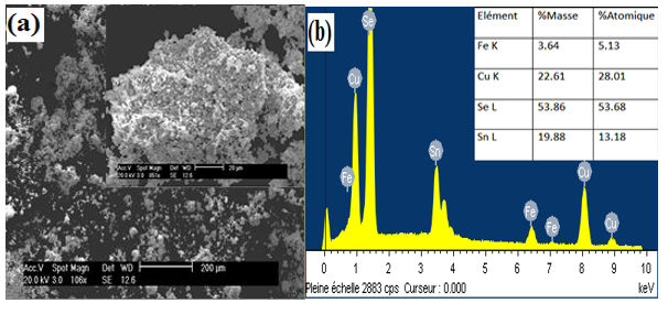 |
| Figure 2: (a) SEM image of CFTSe powder, (b) Corresponding EDS spectrum. |
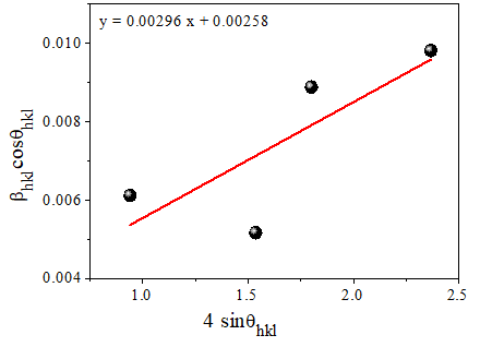 |
| Figure 3: The Williamson-Hall analysis of the CFTSe powder |
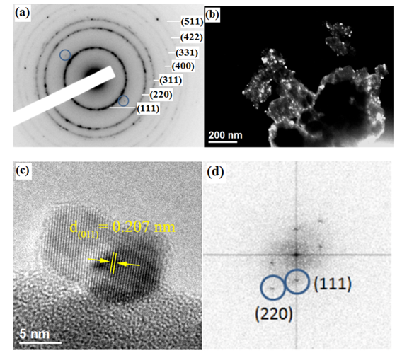 |
| Figure 4: (a) The corresponding selected-area electron diffraction (SAED) pattern. (b) Dark-field transmission electron microscopy image. (c) HREM image of two small grains and (d) The corresponding Fast Fourier transform of the HREM image confirming the presence of Fe grains. |
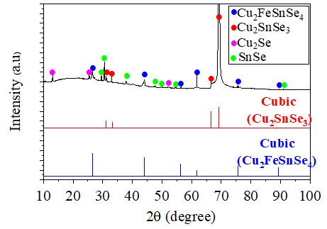 |
| Figure 5: XRD pattern of the Cu2FeSnSe4 thin film |
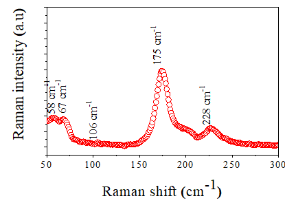 |
| Figure 6: Raman spectrum of the Cu2FeSnSe4thin film |
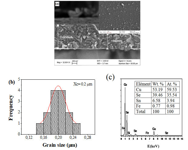 |
| Figure 7: (a) Cross sectional SEM image of the CFTSe thin film, (b) The particle size distributions, (c) EDX spectrum from the CFTSe thin film |
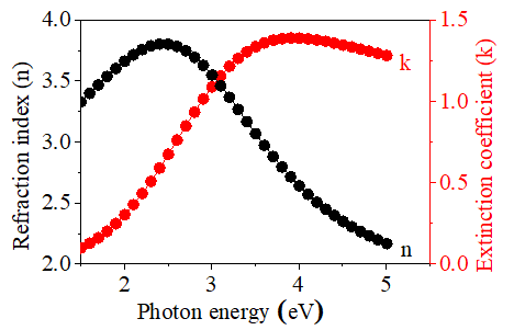 |
| Figure 8: Spectral dependence of refractive index (n) and extinction coefficient (k) for the obtained CFTSe film deposited on Si (100) |
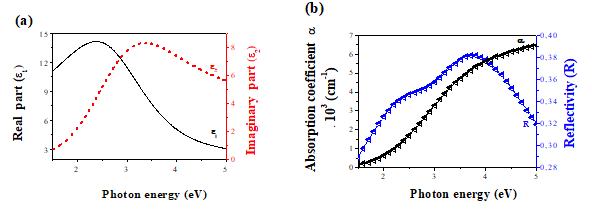 |
| Figure 9: (a) Real (ε1) and imaginary (ε2) parts of the dielectric spectra and (b) Plot of the absorption coefficient (α) and normal-incidence reflectivity (R) with respect to photon energy for the CFTSe film |
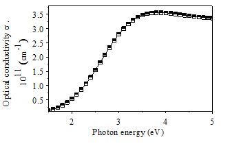 |
| Figure 10: Optical conductivity values (σ) versus incident photon energy for the CFTSe thin film |
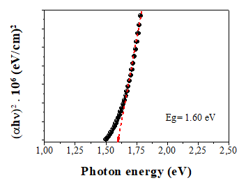 |
| Figure 11: Plot of αhν2versus hν (eV) for the CFTSe thin film |
| Milling time (min) | lattice parameter (Å) | Crystallite size (D) by Scherrer method (nm) | δ (1015) lines / m2 | Williamson’s and Hall’s method |
| D(nm) ε (10-3) | ||||
| 210 | 5.68 | 24.74 | 1.63 | 53.78 2.96 |
Table 1: Structural parameters values of the Cu2FeSnSe4 milled powder


